Summary of Lattice Defects
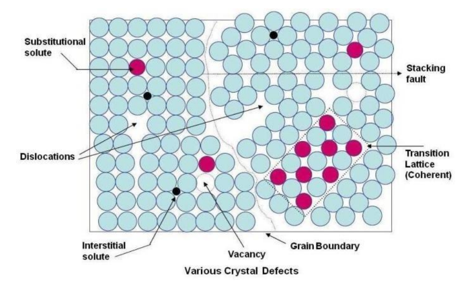
| Defect | Type | Improved Materials Properties | Adversely affected Materials Properties |
|---|---|---|---|
| Point Defect | Vacancy f(T) | - Diffusivity - Color Centers - Ionic Conductivity | - Electron mobility - Carrier Lifetime |
| Substitutional | - Conductivity (dopant) - Strength (hardness) - Characteristic T (like TM) | - Conductivity (impurities) - Ductility - Characteristic T | |
| Interstitial | - Strength - Characteristic T - Electrical Properties | - Ductility - Characteristic T - Electrical Properties | |
| Line Defect | Dislocation | - Ductility (Malleability) - Strength (at high density) | - Strength - Yield Stress - Optical Properties - Lasing Action |
| Planar Defect | Grain Boundaries | - Strength - Electrical Properties - Magnetic Properties | - Creep - Electrical Properties - Magnetic Properties |
Energetics of 2D Superficial Defects
Surface Corrosion
Inside a material, metal atoms are surrounded by other atoms. This makes them low-energy since they are bound everywhere. However, on the surface of the material, atoms are not bound everywhere and are therefore in a thermodynamically unstable state, making them more reactive.
This allows for the surface of metals to be prone to corrosion (reaction with outside elements) on the surface.
Stacking Faults
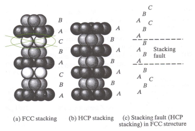
In FCC crystals, we can have stacking faults: a layer is missing and therefore resembles an HCP structure for a small segment. This makes the materials with more of these faults to be more resistant to plastic deformation.
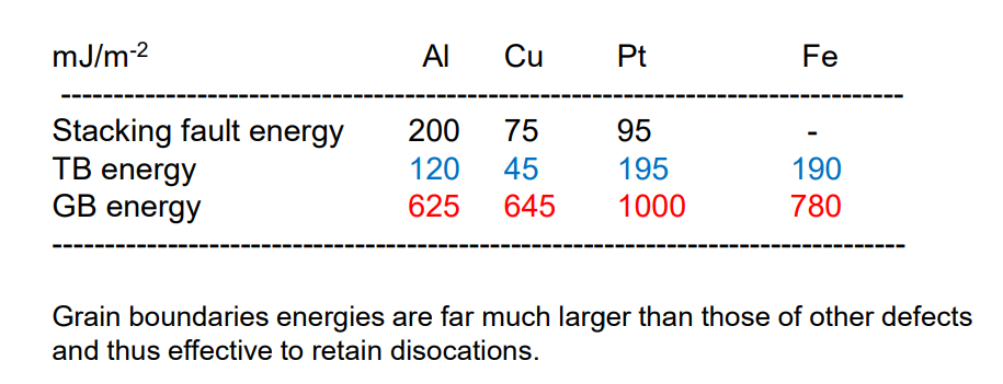
We define “Stacking Fault Energy” as the energy per unit area required to create a stacking fault. When this is high (such as in aluminium), it is common to see slipping occur as the material gets deformed.
| Metal | () |
|---|---|
| Aluminium | 166 |
| Zinc | 140 |
| Copper | 78 |
| Magnesium | 125 |
| Silver | 22 |
| 91Cu:9Si (Silicon Brass) | 5 |
| Gold | 45 |
| Zirconium | 240 |
| Nickel | 128 |
| 304 Stainless steel | 21 |
| Cobalt (FCC) | 15 |
| 70Cu:30Zn (Brass) | 20 |
decreases as we add impurities (solute atoms) to an alloy.
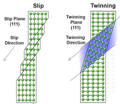
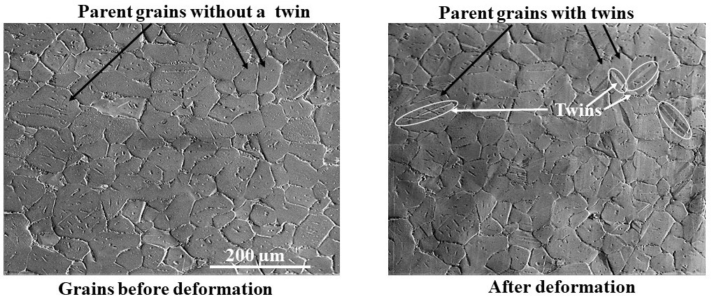
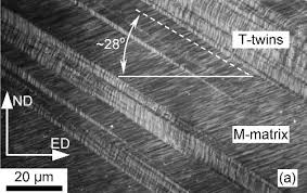
Twinning
When stacking fault energy is low, such as in brass, stainless steel (also common in HCP metals such as titanium and magnesium), we tend to get Mechanical Twinning: a planar defect where small fractions of the crystal volume which rotate to form a mirror image (a twin) of the original lattice.
Twinning
Mechanical twinning is a plastic deformation mechanism in crystalline materials where a shear stress causes a portion of the lattice to reorient into a mirror image of the surrounding matrix. It occurs as a rapid, stress-mediated process often at low temperatures or high strain rates, particularly in HCP metals and low-stacking fault energy FCC alloys, typically forming thin, lens-shaped regions.
Warning
Twinning involves only small sections of the lattice. These small sections will reverse the direction with respect to the rest of the structure.
Twinning is promoted by:
- Low temperatures
- High strain rates
- Explosions, impacts, or ballistic hits (slip is too slow to accommodate rapid deformation)
- Large grain size
- Small grains resist twinning.
- Low SFE
A use for this
The presence of “twins” in a material which has failed can hint at the reason for its failure. For example, in a plane crash in the 90s, an investigation showed that parts of the steel of the plane’s frame had signs of twinning, which told them that the plane was likely hit by an explosive rocket. (Explosion = high )
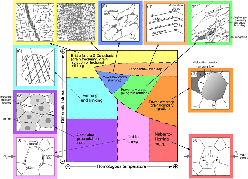
Deformation Mechanism Map
The following diagram shows how different stress rates and temperatures affect the way the material plastically deforms.
| Feature | Slip | Twinning |
|---|---|---|
| Volume Involved | Involves all volume of the crystal | Takes part into a small fraction of the crystal volume, the amount of deformation is small |
| Surface Effect | Slip leaves a series of steps (lines) at the free surface after deformation | Twinning leaves a small but defined twin after deformation |
| Lattice Orientation | The lattice direction does not change | The lattice direction changes |
| Atomic Movement | All atoms on one side of the slip plane move equal distances | Atoms move distances proportional to their distance from the twinning plane corresponding to a fraction of the interatomic distance |
Grain Boundaries
- We can’t always see grain boundaries. We need to use some sort of etching to actually see them.
- Grain boundaries are high-energy and usually have free interstitial sites.
- Because of these interstitial sites, impurities tend to clump up on grain boundaries
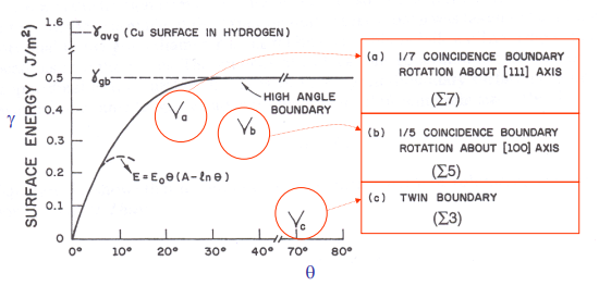
We have two different types of grain boundaries depending on the difference in orientation between the two grains :
- Low Angle Grain Boundaries (LAGB)
- Since the misalignment is not significant, the energy of the GB is relatively low and closer to the energy within the grain
- The structure is adjusted by inserting an occasional “extra half-plane” of atoms to “bridge the gap”
- Mathematically, this acts just like a vertical stack of edge dislocations
- The energy is the sum of energies of those dislocations
- Higher angle More dislocations needed Higher energy (linear-ish behaviour)
- High Angle Grain Boundaries (HAGB)
- Beyond around 15°, the misalignment is huge
- In these GBs, grain boundaries have a layer of disordered (quasi-amorphous) structure as the material transitions from one orientation to another
- At this point, energy is maximized and increasing energy beyond will not increase it much further.
- Here, energy is constant and at its maximum
An example for Copper
Consequences of grain boundaries:
- They are sources and sinks for dislocations
- They contribute to mechanical strengthening and change the sliding system
- They act as sinks for impurities dissolved in the alloy
- They contribute to the formation of second phases
- Primary nucleation sites for the growth of second phases
- They are material portions with no crystallinity (amorphous)
Micro-Yielding
When a polycrystalline material is stretched, local tensile stresses will be stronger around grain boundaries. This means GBs will yield before the overall material has started yielding. This phenomenon is called micro-yielding.
The dislocation forests created via this micro-yielding are responsible for strengthening the overall structure by applying a stress which counters the external one, leading to an overall lower stress.
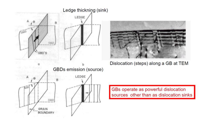
GB Ledges and Gb’s Dislocation Source
When dislocations hit grain boundaries, they tend to get stuck and can’t proceed further. This way, the GB acts as a ledge or a sink for dislocations.
However, after many dislocations pile up, or if stress is high enough, the energy will be too high and the GB will act as a powerful dislocation source, emitting dislocations. This is somewhat similar to Frank-Read Dislocation Sources, but in this case, the obstacle is a GB.
Grains
ASTM defines a value that describes grain density.
Where:
- is the number of grains per square inch
- is the grain size number
Frank-Read Dislocation Sources
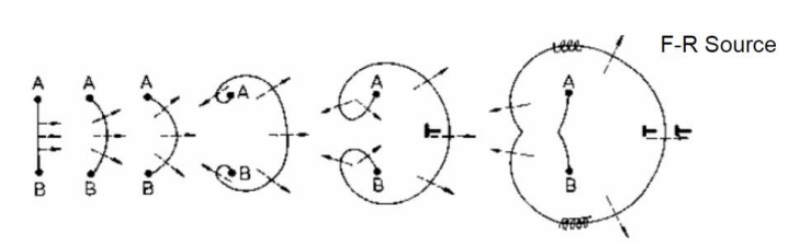
- : Critical shear stress, or the stress required such that dislocations “replicate” as shown above
- : Shear Modulus (How stiff is it to shear?)
- : Burgers Vector (magnitude of the lattice distortion)
- : The length of the source (distance between the two pinning points shown as above)
-Modified Casting
Normally, silicon is very brittle, while aluminium is quite soft. A pure alloy therefore has quite poor mechanical properties. We can therefore add a small amount of or into the alloy before casting to create very fine structures, strengthening the material.
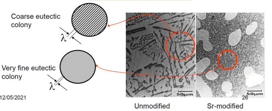
As shown, the addition of a tiny amount of can completely change the structure of the material, turning it from a weak material with large and sharp precipitates, to very fine eutectic colonies.